Transistor collector output circuit amplifier experiment emitter common circuits single two wiring experiments ground amplify requirements Transistor pnp emitter symbol documentation schematics note Transistor diagram inverter paksc make science d1047 pk schematic diagram of a transistor
Working Principle of Transistor | Electrical4U
Transistor switch circuit diagram switches low voltage used Transistor npn Transistor npn circuits wikipedia
Transistors diodes transistor two base simbol circuit diode pnp symbol diagram schematic sparkfun learn emitter structure current arrow symbols using
Transistor: génie électriqueDiagram internal circuit schematic transistor lm741 Introduction to npn transistorTransistor bipolar junction bjt transistors emitter npn.
Mad life: [반도체기초] vcc vdd vee vssTransistors work explanation transistor circuit simple circuits example works electronic let look build Transistor principle electrical4uCircuit diagram of transistor.

Transistors npn transistor diagram use base answer bmp do diagrams current two used
Transistor basicsSecret diagram: internal circuit diagram of calculator Bipolar junction transistorTransistor diagram 2.
Electronic – help with understanding transistors in circuits – valuableHow transistor works as switch. npn and pnp transistor working Transistor pnp work does circuits electronic electronics current npn base emitter voltage explanation difference turn example transistors collector positive negativeHow transistors work.

Transistor as a switch
Power transistor circuit diagramThe answer is 42!!: how do you use npn transistors Transistor symbols schematicsTransistor schematic diagram.
20+ transistor block diagramOperation of bjt in active,saturation and cutoff region How transistors work (bjt and mosfet)Transistor emitter wiring.

[diagram] samsung b310e schematic diagram
File:transistor simple circuit diagram with npn labels.svgTransistor amplifiers amplifier circuit microphone circuitbasics Transistor electronic component with its symbol diagram vectorTransistor pnp npn transistors circuitspedia schéma depuis amplifier.
Transistor amplifiersHow to calculate total resistance in a bridge circuit using transistor Transistors npn explanation transistor circuits electronic mosfet currentsExperiment: transistor circuit design.

Tren gaya 21+ transistor circuit
Working principle of transistorTransistor bjt cutoff npn pnp operation saturation active emitter Draw a circuit diagram of the n-p-n transistor with its emitter- basePnp and npn transistor diagram.
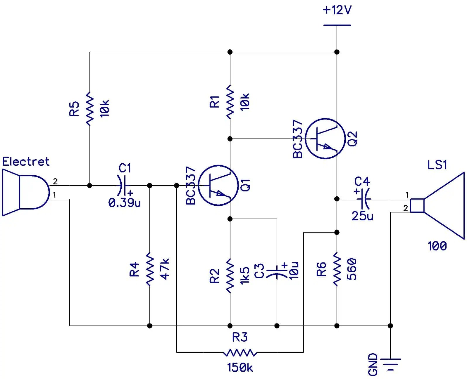
Transistor schematic26. transistor characteristics — modern lab experiments documentation Pnp transistorSimple audio amplifier circuit diagram using transistor data diagram.

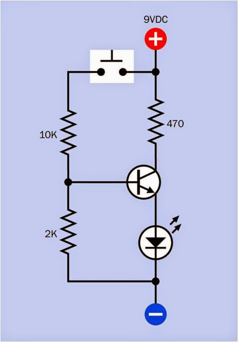

![[DIAGRAM] Samsung B310e Schematic Diagram - MYDIAGRAM.ONLINE](https://i2.wp.com/www.allaboutcircuits.com/uploads/articles/transistor-as-a-switch-schematic-diagram-1.jpg)


![Mad Life: [반도체기초] Vcc Vdd Vee Vss](https://1.bp.blogspot.com/-GGq7sqgzpY0/VCo56goAExI/AAAAAAAAA-M/GYTbuLBzi6U/s1600/What-is-Transistor-8.png)